Making good circuit designs in little time requires an efficient design process. In this section, a given circuit topology is assumed to be optimized — or dimensioned — to achieve a set of target specifications, using a specific technology. Also a short extension into bottleneck identification or roadblock identification is done.
It is assumed that the technology for your transistors, or even the actual type is pre-determined. If this is not the case, then the following discussion can easily be extended to include an extra degree of freedom in selecting the technology or type of transistor.
The most important properties of a MOS transistor in a given technology are a function of just a small set of bias settings/device dimensions that you can set independently:
In general, 3 degrees of freedom can be set independently per transistor. These 3 can be picked from a set {W,L,V GS,V GT ,ID,gm} where the other follow and where many transistor properties follow. Note that e.g. stress parameters and body biasing are not taken into account as (significant) degrees of freedom for the transistor. Typically, V DS is not a degree of freedom to set device behavior but rather only needs to satisfy a minimum value (“voltage headroom”). This voltage headroom V DS and the technology are assumed to be given.
In general, optimizing or dimensioning a given circuit topology for a set of target specifications means finding sufficiently optimum settings for all transistors in your circuit.
If your circuit contains N transistors, this forms a 3N-dimensional optimization problem. And worse, it is a non-linear 3N-dimensional optimization problem. The complexity — or amount of work required — of solving a non linear optimization problem is a strong function of both the dimension of the problem (3N) and of the quality of the starting point for optimization. Speeding up circuit optimization or circuit dimensioning can be done in multiple ways:
Most circuits have some symmetry, in mirrors, cascodes, differential pairs and more. This can be leveraged to decrease the dimension significantly.
After reducing the complexity, leveraging symmetry, the overall complexity can be pushed down quite a lot further. That is discussed below.
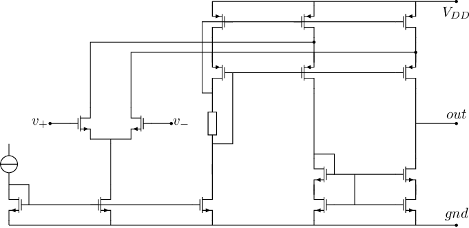
As example, the circuit schematic in Figure 1 is used. This amplifier consists of 15 MOS transistors that are all assumed to work in saturation. Without leveraging the usually imposed symmetry in the circuit, there are hence 315 degrees of freedom. Optimizing the circuit in Figure 1 for some target specifications boils down to an 315 ≈ 14,000,000-dimensional non-linear optimization problem. And that is quite though. And of course that is not what a designer does.
Leveraging symmetry in mirrors and in the diff pair, the 315-degrees of freedom reduce to 36 = 729. The complexity of optimizations and hence the amount of work required for optimization is a strong function of the degrees of freedom. This means that the previously reported 315 degrees of freedom to 36 is a huge improvement. Still, the remaining 36 = 729-dimensional non-linear optimization problem is hard, especially if the starting point for the optimization is not close to the actual optimum.
The complexity of the optimization can however again be reduced significantly. For the example circuit in section 2.3, with 15 transistors, that can be reduced to 6 unique transistors when leveraging symmetry
Typically, optimizing with 3 degrees of freedom (per transistor) can be quite fast due to the relatively low number of degrees of freedom and the associated much lower dependency on initial guesses. On the downside — or upside — it does require that the designer knows the demands on the performance and knows boundary conditions on voltage headroom, current budget, available area and more for each transistor.
Noting that the optimization for individual transistors is quite fast, executing that process 6 times (for the example circuit) is also fast. Optimization per transistor ignores interaction between transistors. This means that per-transistor optimization will yield a decently optimized but not fully optimized circuit. Full optimization must be done using a conventional circuit simulator. However, starting with a decently dimensioned circuit, the final optimizations using a circuit simulator can also be quite efficient.
In linear optimization problems of any size — and assuming that there is a solution — the optimum solution can be found easily. This holds both for numerically solving and for symbolically solving.
Optimizing non linear systems, e.g. dimensioning or optimizing a circuit schematic for a specific set of target performance metrics in a specific technology, is totally different. This forms quite a complex optimization task. To significantly speed up the optimization/dimensioning process:
Getting an as-good-as-possible starting point is mildly important for low-dimensional problems, such as optimizing a single transistor for a set of target specifications for that specific transistor. Doing so, the impact of interaction between transistors is not (well) ensured; for that circuit simulations must be done.
Getting an as-good-as-possible starting point is very important to reduce the time and effort required for optimizing a full circuit in circuit simulators. This is of course due to the many degrees of freedom in the non-linear optimization task to optimize the full circuit. However, the accuracy of the per-transistor optimization determines to a large extent the quality of the starting point for optimizations in circuit simulators, and thereby determines to a large extent the time and effort required for optimizations of the full circuit in a simulator.
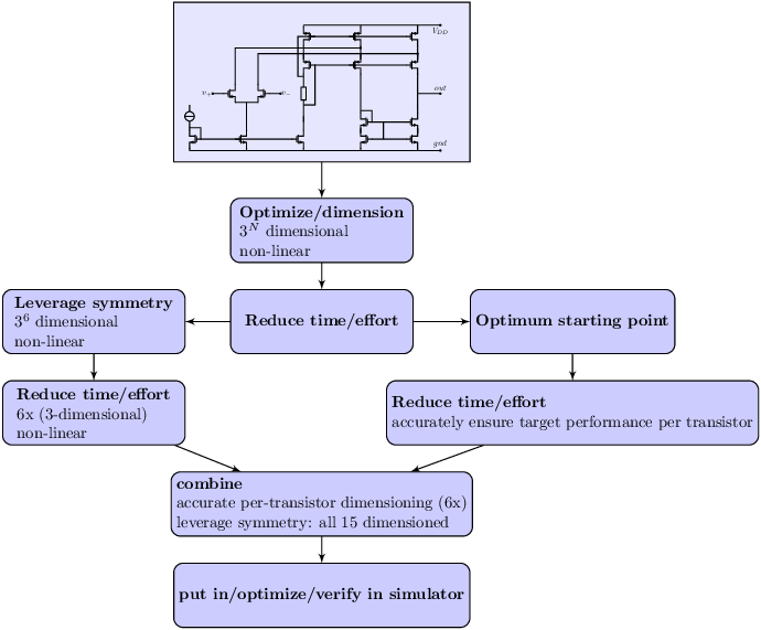
Figure 2 shows a flowchart for efficient optimization/dimensioning of the example circuit in Figure 1. This flowchart can be subdivided into 3 parts:
If the per-transistor approach does not find a decent solution — if target specifications cannot be met for all transistors — there are most likely just a few possible reasons:
In the second case, the per-transistor optimization most likely fails to dimension one or multiple transistors, for the target specifications for those transistors. This indicates a conflict between requirements and design space which hence localizes the likely roadblock for the combination of {target specs, circuit schematic, technology}.