This section recaps the conventionally taught and conventionally used small signal equivalent
models for MOS transistors. After that the (hardly taught and hardly used) correct small signal
equivalent model is introduced. In next sections, these two small signal equivalent
models are used in the context of a very basic amplifier - demonstrating that there
are significant different outcomes for the two small signal models. More precisely: it
shown that the conventionally used equivalent model introduces significant errors.
Conventionally used small signal equivalent
Without digging into it, probably the most widely used small signal equivalent circuit for MOS
transistors is shown in Figure 11. This equivalent is the one that typically is taught in BSc and
MSc courses. In this chapter, this small signal equivalent circuit will be referred to as
SSEC-conv.
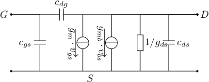
This small signal equivalent consists of 2 voltage-controlled current sources and a few capacitors
and resistors. It can be shown that this model is unable to properly model the behavior of
devices that (fundamentally) have more than 2 terminals.
Proper small signal equivalent
In transistor models, the currents into each terminal are properly described by (elaborate)
equations, yielding

Small-signal wise, this leads to 4x4 small signal parameters as we can get 4 partial derivatives for each terminal current which yields 4x4=16 transconductances
 |
Similarly, in MOS transistor models terminal charges are described as

Small signal wise, we can derive 4x4=16 transcapacitances from the partial derivative of the terminal charges to all terminal voltages as
 |
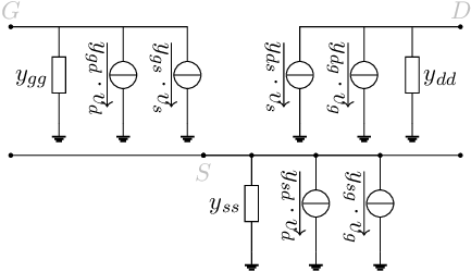
It can be shown that there is redundancy in these 4x4=16 transconductances and in these 4x4=16 transcapacitances. Assigning one of the terminals as the reference terminal, a subset of 3x3=9 cxy-s and gxy-s is sufficient to properly and completely model the small signal behavior of MOS transistors. A further simplification can be done by capturing the 3x3=9 transconductances and the 3x3=9 transcapacitances in 9 (frequency dependent) Y-parameters:
 |
The corresponding (correct) small signal equivalent model for a MOS transistor is then as shown in Figure 12. In this, the body terminal is used as reference node and its terminal voltage is assumed to be the reference voltage (ground). In this chapter, this (correct) small signal equivalent circuit will be referred to as SSEC-Y .
In the remainder of this chapter, a quite simple example circuit is used as vehicle to demonstrate the impact of using (the conventional) SSEC-conv and of using (the correct) SSEC-Y.
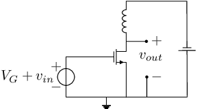
The circuit used is a very basic common source amplifier, with a choke as load (see Figure 13). For this amplifier, an NMOS transistor from a commercial 0.18 μm technology is used, biased at V GT = 0.2 V and V DS = 1 V . OP data as output by the transistor model (BSIM4) for that transistor is used as input for the small signal equivalent circuits.
In this section, equations for the (small signal) voltage gain and (small signal) input impedance are shown when using the widely assumed but incorrect small signal model in Figure 11. As hinted to previously, the results obtained using this model are incorrect but matches textbook derivations. Straight forward derivations now yield for the voltage gain av

whereas for the input impedance it can readily be derived that

The computational workload of deriving these equations by hand increases rapidly with the number of components and nodes in the circuit. Then, using e.g. the MNA matrix to derive small signal properties in equation might be easier. Using the MNA fomulation [MNA][vi] = [excitation] for the circuit in Figure 13 with the small signal equivalent for the transistor as shown in Figure 11,
 |
From this, the (vector) vin, vout and iin as a response to an excitation with magnitude 1 follows from
 |
This yields of course the previously derived
av(jω) = − | (1) | |
zin(jω) =  | (2) |
Numerical values for the used small signal properties in (1) and (2) are copied from the OP data generated for NMOS transistor in a commercial 0.18 μm technology, operated at V GT = 0.2 V and V DS = 1 V . This implies that e.g. the cgs in (1) is directly copied from the 16-transcapacitances listed in the transistor’s OP data. Plugging these OP parameters into the derived equations, Bode plots of av(jω) and zin(jω) can easily be constructed.
Using the (correct) small signal equivalent model in Figure 12, the output voltage of the amplifier follows from directly from applying the KCL at the transistor’s drain node:

Rewriting this readily yields the correct expression for voltage gain:

Similarly, the input impedance follows directly from Y-parameter definition, applied to the input node of the (simple) circuit:

Transistor OP output typically do provide the values of all (9 or 16) transcapacitances in the operating point, but do not report the (9 or 16) transconductances. For the example circuit in Figure 13, we can use
Then the previously derived equation can be rewritten into
av(jω) = − | (3) | |
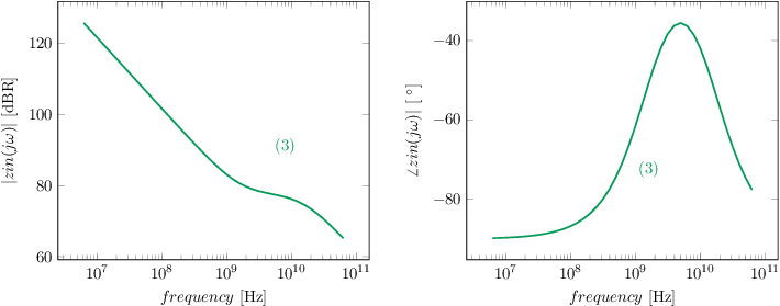
zin =  | (4) |
Plugging (Y-parameter based) OP parameters as provided by a (state-of-the-art) transistor model into these equations, Bode plots of av(jω) and zin(jω) can easily be constructed. For this, the exact same transistor with the exact same biasing as used in section 6.3 are used.
In this section, the voltage gain av(jω) and the circuit’s input impedance zin(jω) as
derived and shown in sections 6.3 (using SSEC-conv) and 6.4 (using SSEC-Y) are
plotted. The same transistor, setting and plugged-in parameters are used, as in those
sections.
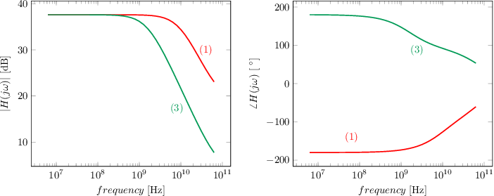
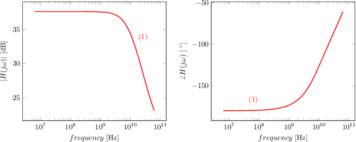
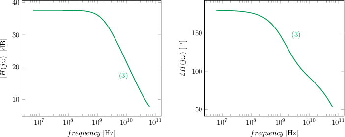
Figure 18 shows the Bode plot for the voltage gains in equations (1), (3). In the Bode plot, the green curves correspond to (3) that was derived by the correct small signal equivalent model and match Spice simulation results (gate leakage is negligibly small). The red curve corresponds to (1) that was derived using the incorrect textbook small signal equivalent; this shows quite some discrepancy with the green curve and with Spice simulation results.
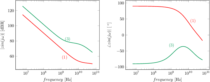
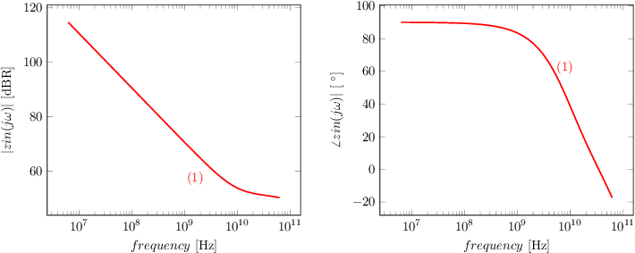
Figure 19 shows the Bode plot for the input impedance of the circuit, as seen from the signal source. Again, the green curves are for equation (4), and these match Spice output. The relation for zin in (2) was obtained using the simplified small signal model in Figure 11; the corresponding curves are shown in red.
For standard MOS models, without any extra passive or active components, the OP data provided by circuit simulators can be used directly. You have to properly use the OP data which is straight forward for transcapacitances and which needs some mapping for transconductances, but that’s it.
![]()
![]()
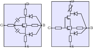
For compound models such as in Figure 20 this is not the case: regular circuit simulators provide only the OP data (including the small signal properties) for each instance in that subcircuit, individually. The OP data from the individual components in a compound model are not directly usable in derivations. Of course you could construct your own elaborate small signal equivalent and plug that one in e.g. the CSC of Figure 13 but the resulting derivation is then quite a lot more complex and — much worse — the resulting equation is then most likely far too big to interpret or to use for syntheses purposes.
ProMOST handles compound models, and derives a full set of equivalent small signal parameters for the total compound model. This is done by running DC, OP, noise and Y-parameter analyses in tandem. ProMOST then outputs
These equivalent OP and noise data properly describe the behavior of the total compound model. Using these equivalent OP data properly in your small signal model ensures high accuracy AND retains simplicity of derivations/equations to a maximum. This can be leveraged to design better circuits in less time, and to get better insight into the transistors.